The aim of the this programmer was principally to program the PIC 12F629. But as the PIC 12F675, PIC16F630 and PIC16F676 have same electrical and logical programming interface, I have extented the compatibility to these 3 PIC models.
Their are many PIC 12F629 very simple programmer but all required a separate power supply. The smarter ones are taking it from the PC through a USB connector. Though I wanted to get rid of this second connector to make the easiest programmer for the PIC12F629.
When using WxPic it is compatible with the JDM(2) adapter for serial port. Use this adapter selection to operate the F629 programmer.

F629 programmer
Schema

The F629 programmer Schema
The problem to solve for programming the PIC12F629 without external power supply is to build 2 supply voltages (+5 and +13V) and to be able to raise the +13V before the +5V. Most of the components in this schema are dedicated to this purpose.
To get 13V from the serial port it is not possible to use the ground of the interface as the 0V reference. It is necessary to use the negative voltage produced by the interface. So the VSS of the PIC will be set to -5V from the interface GND. This negative voltage is produced throught the PIC clamping diodes when the RTS (clock) or CTS (data) are brought down and regulated by Z1. The PIC12F629 clamping diodes accept up to 25mA wich is more that what the serial port can produce. Therefore, without installed PIC the supply voltage cannot be produced. C1 allows to keep the 5V while the clock and data are high.
The 13V is then easy to produce: TxD will be clamped to 8V by a 7.5V zener in serie with a diode. The diode is necessary to allow to drive TxD to VSS without being clamped to the ground by the direct current of the zener.
The PIC VDD cannot be connected directly to the ground because the PIC12F629 requires that 13V raises few microseconds before 5V. This means that during these microseconds VSS is -5V, GP3 (VPP) is +8V and VDD must be -5V. The role of Q1 is to connect VDD to the ground after VPP has raised. The few micro-second delay is obtained by C2 discharging. A FET transitor is necessary because the current though the VDD pin may go in both directions. Usually it enters in the PIC but when clock is high, its clamping generates a current output from VDD.
This VDD output clamping current is an issue when Q1 is blocked. It prevents VDD to stay low as it should, it could event raise the voltage on VDD higher than GND with a risk of overflow of maximum VDD. Q2 is dedicated to avoid this issue by disconnecting the clock input from RTS when Q1 is blocked.
Q3 is used to adapt the voltage range between the PIC data pin [-5V, 0] and the interface approximatively [-5V, 5V] in both direction. It is used in common based mode. The emitter and collector roles are reversed when it is the interface that drives the data.
R2 is used as a pull up when the PIC drives the data, and transmits the signal in the other direction. To improve the signal quality that must reach -5V at low level, D2 limits the loss of negative voltage that may occur through R2. It helps when the interface has a limited voltage range. But it may be omitted with a compliant RS232 interface.
Printed Circuit Board

The F629 programmer PCB viewed from copper side

The F629 programmer parts viewed from component side
The figures above describe the PCB for the programmer. To print these document in actual size the following pdf files should be used. Note that the PCB in the pdf is provided viewed from the component side. This allows to print it and used the printed sheet as a mask with the printed ink touching the photosensible coat.
The main copper area is connected to the ground. Remember that this ground is not the PIC VSS. As you can see I like to maximize the ground plan. Though this is not a high frequency device that would require a ground plan, I reduce the use of ferric chloride.
Note that the PIC socket is mounted on the copper side. The 5 pins that must be soldered have a large pad outside of the circuit to help that operation. A 14-pin socket is used, though the PIC12F629 needs only 8, to accomodate properly the PIC16F630 and PIC16F676. Take care to mount the socket in the right direction in order that you get the right indication of the PIC mounting direction. The half circle on the PCB should help you to find the right direction.
The mounting of the PIC must always put the Pin1 in socket's pin 1, for a 8-pin or 14-pin PIC.
Mounting
To fit in a small box the components have to be mounted close to the board. The transistors must be inserted the closest as possible. The electrochemical capacitor has to be laid on the reserved place.
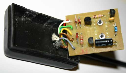
The mounting of the components
The soldering is easy except for the integrated circuit socket. I have reused an old socket that has the advantage to be fixed with 2 screws diam 2mm. This avoids to force on the soldering when inserting and especially removing the PIC while soldering on the copper side reduces the resistance of the assemblage.

The socket on soldering side
The indications on the PCB should help you when soldering the cable coming from the DB9 (the higher mistake risk in this realisation is there). To help again in this direction below is the DB9 RS232 pinout for our 5 signals viewed as you will see it when you will solder the wires to the pins (either the front view of the male connector or the rear view of the female connector).

The RS232 DB9 connector from the rear of the female connector
Original Source : WxPIC
Download Software :
Hello,
ReplyDeleteI'm Trying to contact you but i can't find any email address.
please contact me via my email:
erancen (at) gmail.com
Thanks!